
Silicon is currently the foundation of modern technology, but it has limitations as a semiconductor. While it facilitates easy flow of electrons, it is not as receptive to holes (positively charged electrons) which are crucial for some types of chips.
Furthermore, its heat conductivity is low, leading to frequent overheating issues and the need for expensive cooling systems in computers.
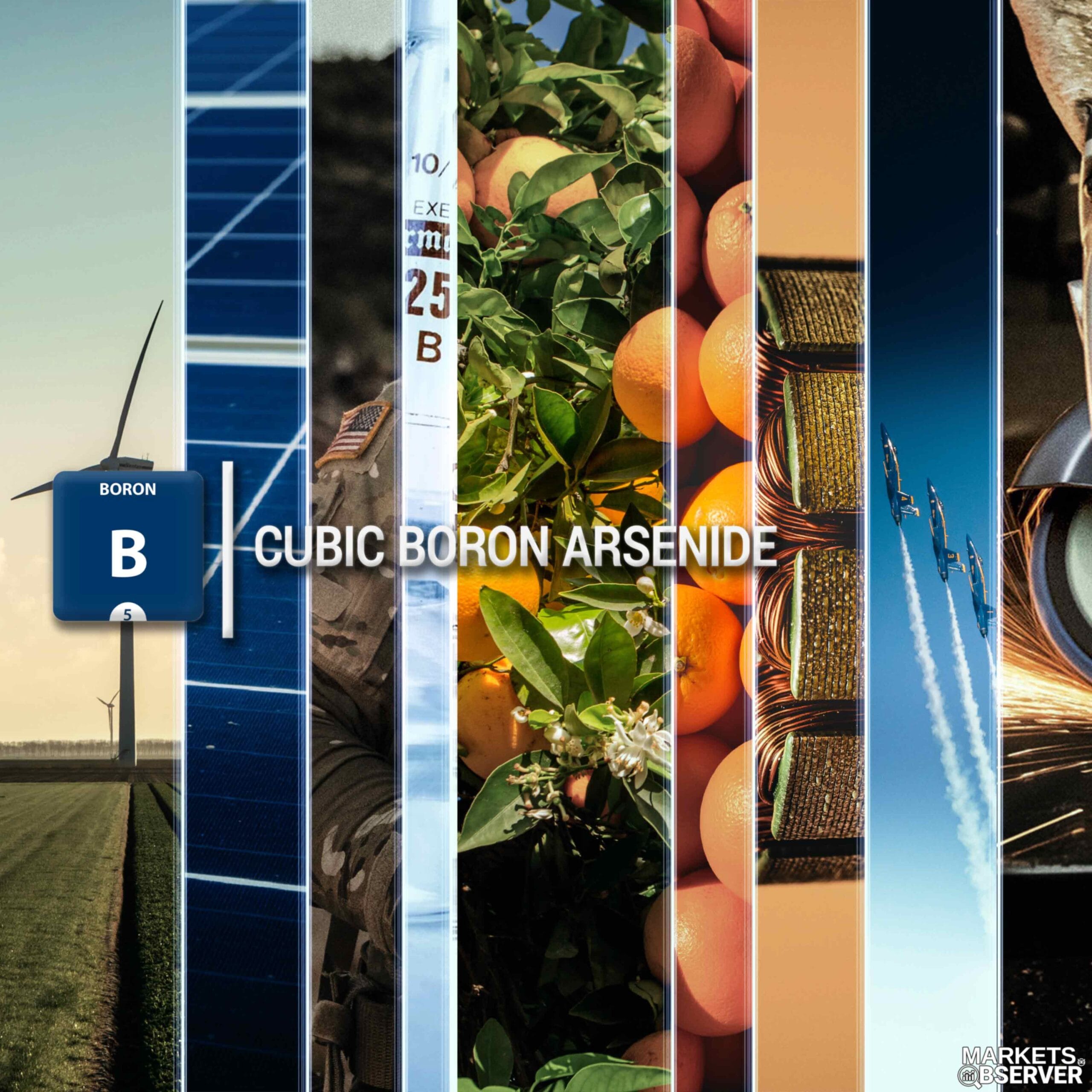
One of the most promising candidates to outperform silicon is cubic boron arsenide (c-BA).
In this article, we will explore recent CBA research and potential applications of c-BA, and how it might play out as replacement to silicon as a leading semiconductor.
- Cubic Boron Arsenide has the potential to outperform traditional silicon semiconductors
- Cubic boron arsenide has the third-best thermal conductivity of any material, behind only diamond and isotopically enriched cubic boron nitride.
- The high thermal conductivity makes CBA an attractive material for heat dissipation.
- C-BA has good electron and hole mobility, which is important for semiconductor devices.
- C-BA has a good bandgap, which means it can potentially be used in a wide range of electronic and optoelectronic applications.
- C-BA has been shown to be stable at high temperatures, making it suitable for use in high-power electronic devices.
- Researchers are still exploring the full potential of c-BA and working on improving its synthesis and processing techniques.
- So far, only lab-scale batches have been made but pending research could prove its economical viability as a replacement for silicon in the near future.
Cubic Boron Arsenide is rapidly becoming the favourite next-generation semiconductor material, offering improved performance and heat dissipation over silicon.
One of the most important properties of c-BA is its high thermal conductivity, which makes it an attractive material for use in high-power electronic devices.
C-BA has a thermal conductivity almost 10 times greater than that of silicon, and is only surpassed by diamond and isotopically enriched cubic boron nitride.
Another important property of c-BA is its good electron and hole mobility.
Unlike silicon, which is good for electron mobility but not for hole mobility, c-BA has good mobility for both electrons and holes (positively charged electrons).
This makes it an ideal material for building high-performance semiconductor devices.
C-BA also has a good bandgap, which is an important property for semiconductor materials. The bandgap determines the energy required to move an electron from the valence band to the conduction band.
C-BA’s bandgap is similar to that of silicon, which means it can potentially be used in a wide range of electronic and optoelectronic applications.
One of the challenges of using c-BA as a semiconductor is its synthesis and processing. The material is difficult to synthesize and process, which has limited its widespread use.
However, researchers are making progress in improving the synthesis and processing techniques, and are exploring new methods for producing c-BA with better quality and purity.
Heat dissipation in high-density devices
Cubic Boron Arsenide’s superior thermal conductivity makes it a viable solution to the problem of heat dissipation in high-density devices.
With electronic components becoming smaller and more densely packed, efficient heat dissipation becomes increasingly important to prevent efficiency and safety issues.

Cubic Boron Arsenide as a potential material for photovoltaic and light detection applications
Cubic Boron Arsenide’s transport properties of photocarriers could make it a suitable material for photovoltaic and light detection applications.
This, coupled with its improved charge mobility and thermal conductivity, gives it an edge over silicon and other semiconductor materials.
Heat is already causing silicon to be replaced for power electronics
Silicon carbide is replacing silicon for power electronics in major EV industries including Tesla, since it has three times higher thermal conductivity than silicon despite its lower electrical mobilities. Imagine what boron arsenides can achieve, with 10 times higher thermal conductivity and much higher mobility than silicon. It can be a gamechanger.[2]
Jungwoo Shin via MIT News Office
Cubic boron arsenide could end up outperforming silicon carbide (SiC), gallium nitride (GaN), gallium arsenide (GAs), and graphene for power electronics in the long run.
New work confirms a unique combination of both high mobility for electrons and holes in Cubic Boron Arsenide
- Researchers from MIT and the University of Houston have conducted experiments demonstrating the potential of cubic boron arsenide as a next-generation semiconductor material.
- The team confirmed that it has high electron and hole mobility, and thermal conductivity nearly 10 times that of silicon.
- They used optical detection methods and ultrafast laser spectroscopy to validate earlier theoretical predictions.
- Despite remaining challenges in large-scale production, the material shows strong potential to outperform silicon and gallium arsenide.
Early theoretical work[3] was followed by experimental confirmation across three 2018 studies[4][5][6].
Now, experimental proof confirms the long-hypothesized high mobility for both charge carriers in c-BAs[2].
The groundbreaking method that made the study of Cubic Boron Arsenide possible
The team combined crystal growth expertise with femtosecond ultrafast laser imaging to capture energy and charge transport dynamics using scanning ultrafast electron microscopy.
The exciting discovery: Cubic Boron Arsenide’s persistent “hot” electrons
Researchers found that hot electrons in c-BAs persisted longer than in conventional semiconductors. This behavior is tied to the same property that enables high thermal conductivity. Longer-lived hot carriers mean more efficient energy harvesting — a huge plus for solar cells and advanced optoelectronics.
References:
- “High Ambipolar Mobility in Cubic Boron Arsenide” , Shin, Jungwoo. MIT News Office, 2022.
- “Thermal Conductivity of Cubic Boron Arsenide” , Lindsay, Lucas et al.. Physical Review Letters, vol. 111, 2013, p. 025901.
- “Experimental Realization of High Thermal Conductivity in Cubic Boron Arsenide” , Kang, J. S., et al. Science, vol. 361, no. 6402, 2018, pp. 575–578.
- “Thermal Properties of Single-Crystal Cubic Boron Arsenide” , Li, Wu, et al. Nature, vol. 561, 2018, pp. 385–388.
- “High Thermal Conductivity in Cubic Boron Arsenide Crystals” , Zhou, Y., et al. Nature, vol. 561, 2018, pp. 373–377.